 DYNALAS
MiniLED Reflow
MiniLEDs are common in consumer electronic goods such as TVs, monitors, laptops, and smartphones as well as automotive displays, signage and LCD backlights. Due to the high component density and small size, it is critical that the process to solder joints is done without causing damage to sensitive components.
All our solutions come with closed-loop controlled power, uniform top-hat profile, and a wide range of spot sizes, including circular, ring, square, rectangle, to precisely meet your application needs.
Our laser systems offer 3 distinct advantages:
1.Precise temperature control.
2.Uniform and shaped laser spot.
3.Adaptive spot size
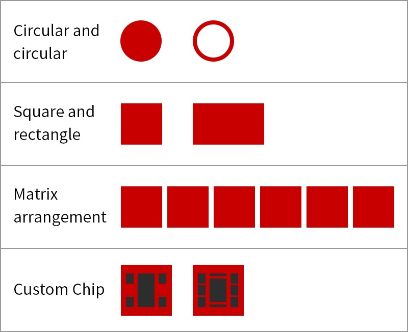
We offer various shapes of light spots – square, rectangular, circular, and circular.
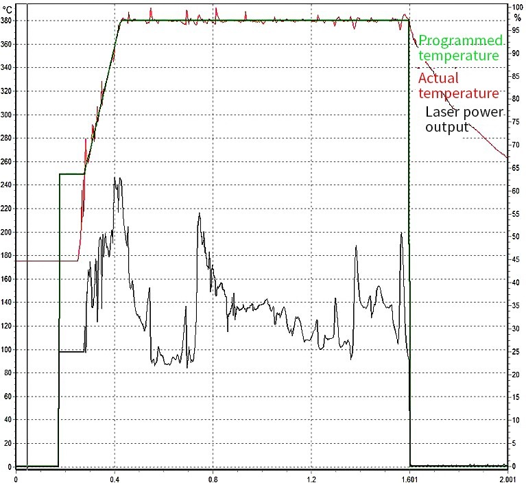
The figure shows that the laser system changes the laser temperature through high-speed closed-loop control of the pyrometer feedback, achieving the predetermined temperature curve.
Compared with traditional convection reflow ovens our lasers offer several advantages:
- By precisely controlling the amount of power and its target it reduces the risks both of overheating the targeted component and damaging sensitive nearby elements.
- Rapid heating and cooling reduce the risk of thermal damage and warping of components leading to higher quality results.
- Non-contact process reduces the risk of contamination and damage to sensitive components and surfaces.
- Precise, and efficient heating improves overall energy efficiency.
- More compact assembly save a significant amount of space in the production area.
- Wider use of applications as it can be used for more substrates allowing for finer pitch applications, a trend likely to continue as PCBs becomes increasingly dense.
MiniLED Rework
MiniLED rework is a necessary step as a consequence of damaged miniLED components during the reflow process requiring repair. Some possible failure states are solder joint defects, misalignment, tombstone, and burned boards.
There are two heating processes in the miniLED rework process.
Firstly, the faulty component must be removed from the PCB using heat.
Secondly, after cleaning the site to ensure proper solder joint formation a new miniLED, or alternative component, is placed in the desired location and soldered to the PCB using heat.
To address this need we offer both standard tools, such as our standard rework laser system, as well as a specially design dual spot system which can individually adjust the power in each beam while avoiding to damage the board between the joints.
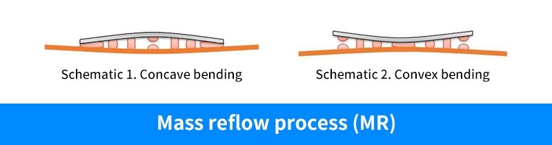
High thermal stresses results in bending which causes 3 types of poor quality solder joints:
①Non-wet joints. Seen in schematic 1 edges and 2 middle.
②Streched joints. Seen in schematic 1 and 2.
③Bridge joints. Seen in schematic 1 middle and 2 edges.

Low thermal stresses results in healthy joints.
MicroLED Reflow
MicroLED is a ultra-small, light-emitting diode display technology with individual pixel sizes in the micrometer (µ) range (each LED size technically below 100µm). This emerging technology produce brighter and more vivid colours, enhance contrast, at higher energy-efficiency and longer life-spans than current technologies like OLED and miniLED. It is also possible to manufacture flexible displays and integrating sensors, such as fingerprint readers, opening up a world of possibilities.These advantages make it attractive for high resolution large-scale video displays, virtual (VR) and augmented reality (AR) headsets, and other wearable devices.
All of our Micro LED reflow solutions can achieve a spot size of up to 50 μ m, and can adjust the size and shape of the spot; Simultaneously equipped with an ultra high speed closed-loop control pyrometer to achieve closed-loop temperature control, combined with unique optical shaping technology, the size of the light spot can be controlled within a precise range, the energy distribution is highly uniform, and precise temperature control can be achieved within a very small range.